From blinking a simple LED to the protocols like UART, and SPI, digital systems require clocks of multiple speeds for implementing different logic.
The FPGAs have limited external clock inputs from the clock generators. Let's assume we have a single clock of 100 MHz from an external crystal. Now the question arises: How to generate multiple clocks using 100 MHz?
Clock Division Using Registers
A simple divide-by-2 logic using flip-flops/counters can be used to drive a 50 MHz clock from a 100 MHz clock. The good aspect of this approach is that It's very simple to implement but has many hidden disadvantages.
Disadvantages
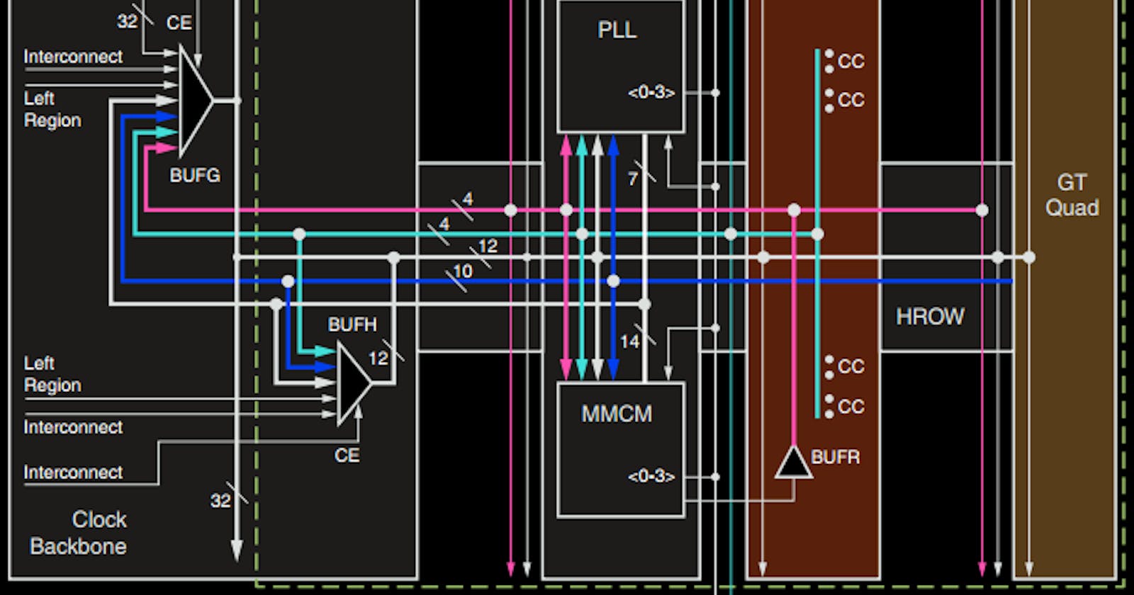
The clock should reach all registers at the same time (minimal skew), this eases the timing closure and increases the overall performance of the FPGA. In order to provide the clock FPGAs have dedicated clock routes and networks, some of them are local (in a particular region of the chip) and some are global (can reach all regions of the chip).
These dedicated clock routes have high fanout, high slew, lesser skew and minimal jitter. However in the case of clock division using registers the clock is generated using the logical elements which generally have lower fanout, more jitter and skew.
Lower Fanout
The clock path should have higher fanout as it needs to feed a large number of logic blocks in the chip. However, the clock routed through logical elements generally has lower fanout which may deform the clock signals resulting in poor clock quality and ultimately poor design or indeterministic results.
Skew
The clock should reach the logical elements with minimal skew and fixed latency. Clock routed through logical elements has variable latency and larger skew, in other words, the clock reaches different sequential elements at different times thus producing uncertainty in the output of the design.
Jitter
Low clock jitter is essential for the integrity of high-speed signals. The dedicated clock routes are designed to keep the jitter at a minimum.
Good Practices for Clock Division in FPGA
Dedicated Primitives
Most FPGAs have dedicated PLL/MMCM which can be used to generate a divided clock. Dedicated global buffers may also be used for the said purpose. The clock generated using these methods will be routed with the best clock properties (jitter, skew, slew, fanout).
This approach reduces the portability of the design to some extent.
Clock Enable
Instead of dividing the clock, the clock enable approach may be used. For example, we want to generate 50 MHZ from a 100 MHZ clock, instead of diving the clock, generate a triggering pulse after every other cycle (50 MHz) and use this triggering pulse to drive the registers in the 100 MHz core clock.
One of the advantages of this approach is that the entire system is on one clock resulting in simpler constraints. However, in the larger designs where the enable signal has a high load the routing time may increase as this approach uses flip-flops with enable pins.
Clock Network in ASIC vs FPGA
The clocking mechanism in ASICs is totally different from the FPGAs. In ASICs there are no dedicated clock routes, PLL etc. The clock network needs to be planned and created by the designer changing the whole story.
Feel free to reach out:
